
Vent Vias
Exposed vias can introduce a number of potential issues during the circuit board assembly process. Tenting vias (covering them with solder mask) is a quick, easy, and free way to eliminate these potential issues.
Visibility
Exposed vias make visibility a challenge. All of that exposed copper may look like a potential defect to an inspector. By covering these vias, it’s much easier to focus in on the real solder joints and not be distracted by all that noise.
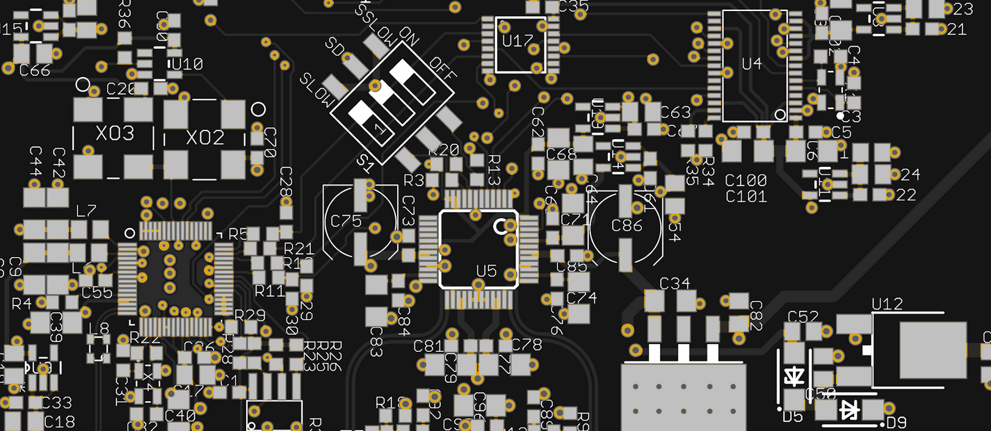
A high number of exposed vias can be disorienting for inspectors
Silkscreen Legibility
Whenever there’s a high number of exposed vias, the PCB fabricator is required to cut your silkscreen lines, since silkscreen will not stick to the vias. This makes identifying the location of devices, and most importantly, the polarity of devices very difficult.

All of these exposed vias not only make visibility difficult, they also contribute to silkscreen getting cut off
Contrast the above image with the image below. Notice how much easier this design is to look at, and how much easier it is to identify polarity and locations of devices.

This design may have problems, but exposed vias isn’t one of them
Risk of Bridging
There’s also a fairly high risk of solder bridging with exposed vias. If the vias are too close to certain devices, the solder could easily jump from the pad it belongs on, and bridge across to the via it does not belong on.

Solder could easily bridge to these vias that are on different nets
In short, please tent any vias that are not used for testing purposes. Your manufacturer will thank you for it.

Vias not used for testing are tented. Silkscreen can be printed right on top of them.